Category Archives: hardware

SiLabs EFM32 Happy Gecko starter kit – first impressions

More unboxing. It includes a CR2032 coin cell in the box. Handy when the product line’s premise is ultra low power. It includes two usb cables, one mini, one micro. What the hell. why are you using mixed connectors?! (One for debug, one for user, similar to the original STM32F4 discovery)

Nice looking board, nice screen. Factory demo software is space invaders! Nice demo of touch buttons, physical buttons and the screen. Startup screen shows the debugger state as well. Expansion header seems to have a full silkscreen with correct positioning. Debug connector for connecting your own debug hardware is the full ARM Cortex with trace header, 2×10@1.27mm pitch. This is somewhat unusual, I’ve never had one that broke out the full ETM pins.

The kit user guide implies that there’s a USB flash drive in the box, containing simplicity studio. Thankfully that’s not the case. That would have been really wasteful. (Yes, yes, helpful for some people with shitty internet, but incredibly wasteful for everyone else)

The onboard JLink OB also presents a mass storage device, with a (broken) mbed link, a link to the starter kit’s home page, and a link to simplicity studio’s homepage. Rather shitty filenames, but I guess that helped someone’s day :) Bit lame about the mbed link not working though. It looks like something that mbed setup to be permanent, but someone overlooked somewhere: http://mbed.org/device/?code=200501120000B7A4D74B847B (Update: It might actually work, but mbed’s website was hacked at the time of writing….)

The rest of the kit user guide doc is rather sparse, (to be polite) simply containing some screenshots of how to run demos and get more information from within Simplicity studio. The kit home page does have a link to download the schematics though, that’s nice.

Doesn’t work with OpenOCD at the time of writing, but very basic preliminary support is proposed in http://openocd.zylin.com/#/c/2931/
Atmel SAMD10 Xplained mini board review

Got a pile of dev boards for some testing. Some first impressions of the ATSAMD10-XMINI. First off, it’s nice and cheap, $9 or so. Comes in a really small cardboard box, with absolutely no documentation beyond some links on the box. Totally fine, no need for anything else these days. The board is a somewhat unusual shape, with the micro usb connector for the onboard DDBG (CMSIS-DAP) protruding out the back. Whatever. At first glace, the board appears well labelled. A closer glance….. well…

The user guide for this board refers to all the headers as JXXX. The J number is NOT in the silk on the board. The userguide has a picture of the board, and marks some of the J headers, but not all. The rest you have to just sort of figure out. This seems like a really amateur oversight. Fixing the silk would have been ideal, but at least the documentation could have a better overview of the board! (The userguide does manage to include screenshots of how to install atmel FLIP, which seems like a total waste of space for this document)

The user guide refers to the pins with J200-1, -2, -3, etc. The silk on the pad arrays is just numbered 1..5, and A..P. There’s silk on the back describing some pins, no idea why some and not others. There’s a big box of silk on the back that seems to be describing some pins, but no idea which, or what order.

There’s a specially boxed off section of pads in the top right, 2×10. It’s unlabeled. No idea what it’s for. (Update, turns out this is for Xplained Pro addons, the userguide covers this, and actually uses the grid array notation that matches the board.)

The user guide does (un)helpfully include arduino pin numbers, for the arduino compatible pin arrays, but there’s no mention of arduino software, or linked anywhere, so who cares about that. The column in the table that includes this is unlabeled as well.

The factory firmware is a morse application. Connecting to the CDC-ACM uart provided by the EDBG module lets you blink out letters, and tapping in keys on the user button prints them to the uart. It resets every few seconds idle and prints some help text. Neat enough.

The user guide does NOT include the schematic of the board. This is a serious omission. Particularly given the poor documentation/silk screen match up, but also as these boards are often used as examples for your own projects. A snippet of the power supply section is included, but again, the labels don’t match the board. I went back and forth through the user guide a few times to make sure I wasn’t missing anything. However, the software package download, which I skipped initially, actually includes no software. It includes all the schematics and proper board diagrams that should have been in the user guide. Pretty poor form Atmel :|

No comments on the tools or device itself yet, that’s for a much later date :)

Terminus Tech 7 port usb 2 “high speed” hub teardown

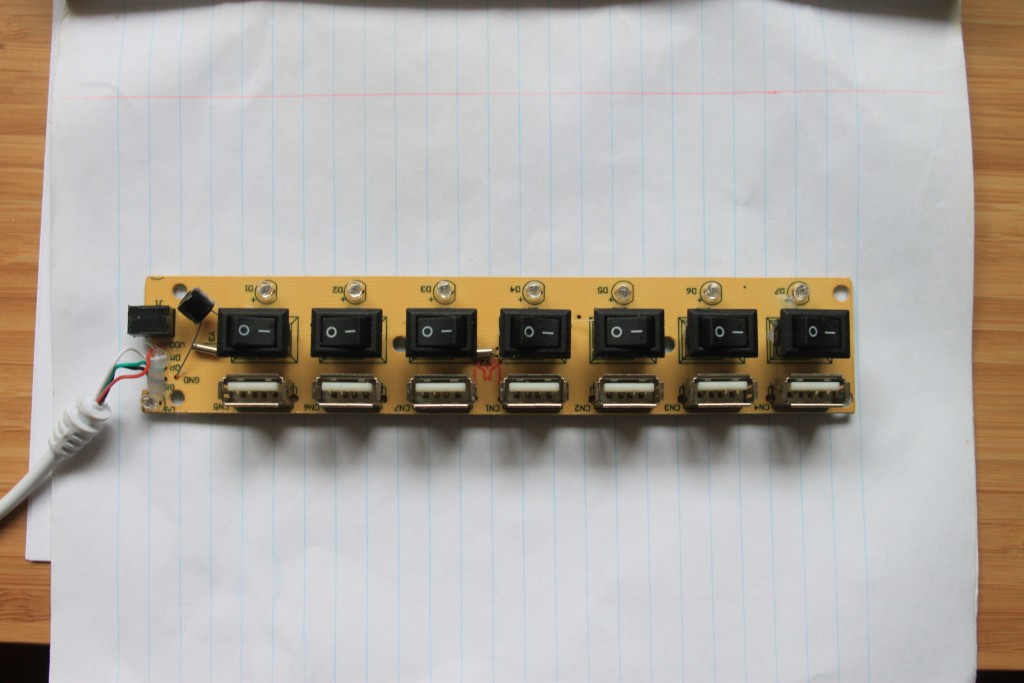
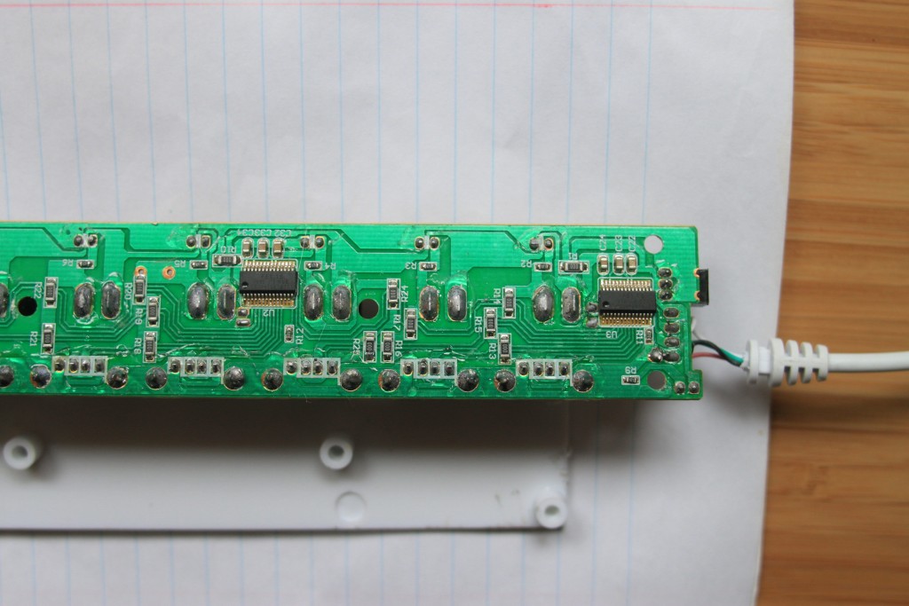
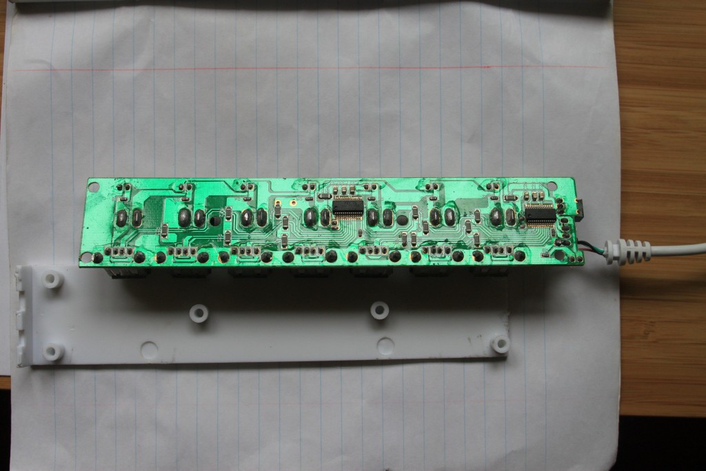
7 port usb 2.0 “high speed” hub, with per port power switches and leds. Only shows up as full speed in lsusb. Leds on ports are very bright, power switches only cut vbus line, rather flaky construction, shaking or bumping can cause disconnects. Seems to consume too much power, without external 5V (not included) vbus can be very low. Available on ebay, tmart, dx.com… http://www.ebay.com/itm/371304833792

The fe1.1s chips are meant to support high speed, so…?

Update: When I had it open, connected to a different computer, it showed up reliably as high speed. Back on the original computer, disassembled, still high speed. Case closed up again, it would show up normally as full speed fallback, and only occasionally as high speed. Further testing indicated that the front panel usb socket is the actual cause. Connecting this hub to another high speed hub showed up reliably as high speed.

The sexy input cap is 200uF, 10V. The rocker switches are KCD11, rated 3A 250VAC, or 6A, 125VAC! The crystal is umarked, but must be 12Mhz from the datasheet.

2015_06_17-14_30_42--img_9408_JFR

2015_06_17-14_30_37--img_9407_JFR

2015_06_17-14_30_00--img_9406_JFR

Carlo Gavazzi EM210 coupled display panel teardown

The Carlo Gavazzi EM210 series [1] of 3 phase energy meters have a rather neat feature. You can mount them on a DIN rail or panel mount, with the same unit, and the display portion is simply detachable, and plugs back in on the reverse side. This is neat tech, and probably saves on inventory in a few distributor places at least, though I don’t imagine it makes any real difference for the end user, who will mount it once and leave it. Still, the display piece has the control buttons and the LCD display, no batteries, and no contacts. So I pulled it apart :)

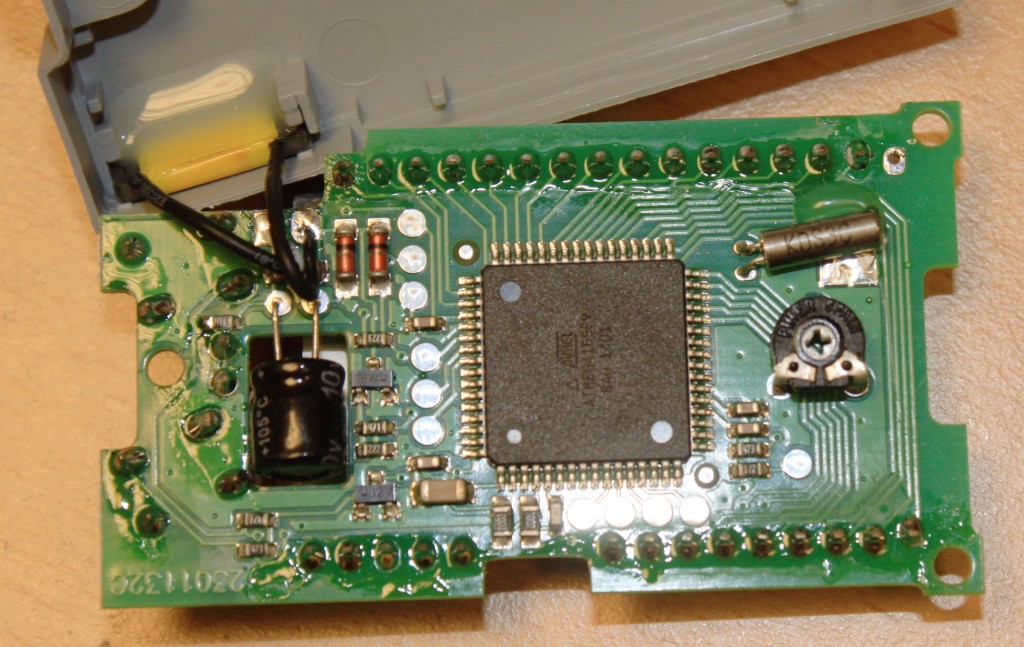
I don’t know how it works really, it’s presumably the same method as NFC, by modulating the power draw from a capacitively or inductively coupled connection. It’s cool though. ATMega169 for the LCD control and buttons. Not entirely sure what the crystal is for, it’s marked “KDS3C” but I didn’t look further for a speed marking. Presumably you need a proper crystal to be able to synchronize the coupled connection properly? I don’t believe it’s an RTC crystal, as this is the detachable display portion. I always like seeing cutouts mid PCB for inserting big components.

The trimpot is an interesting idea. It’s used as a “lock”. With it turned all the way one way, the device is considered locked, and this screw access is on the back of the display portion. This portion also has tags for tamper seals, so I guess that’s one way of doing it on the cheap? Presumably just an ADC input to determine lock status.

The oddly slanted through hole parts on the left are the front panel buttons, nice alignment :)

ATMega169 for LCD control, coupled connection

ATMega169 for LCD control, coupled connection

[1] I’d link to them, but their website is junk and doesn’t let you link to products, and requires sign up to get a datasheet, that uses old names. The same sort of stupid games with redirecting you to different websites for different markets for the same device and all the usual terrible product management choices that lead engineers to ignore your products.

minix neo x5 mini – backup partitions and investigate

Urgh, I hate the massive pile of rom noise around anything to do with android devices.

I’m using https://github.com/neo-technologies/rkflashtool because it appears to be actually maintained. https://github.com/linuxerwang/rkflashkit is also somewhat convenient, though it’s gui only. If it was a nice python tool with a gui front end that would be even better. (no idea why you need waf and install either, simple “python run.py” is perfectly suitable.) libusb+python is perfectly acceptable for this sort of thing. No idea why people went straight to C code. https://github.com/neo-technologies/rockchip-mkbootimg looks good too, but I’ve not poked it yet. Anything that’s being maintained basically.

A commonly referred tool, https://github.com/naobsd/rkutils while often pointed to, is effectively a dead end with zero follow up commits. I’ve no interest in following that nest of forks.

Anyway, here’s the bits that actually worked to open up the boot partition image extracted with either rkflashkit or rkflashtools…

  • ./rkflashtool r boot > boot.img
  • dd if=boot.img of=bootimg.gz skip=8 bs=1 count=20000000
  • mkdir hohoho && cd hohoho
  • gunzip < ../bootimg.gz | cpio -i --make-directories

According to this review of boot.img formats, this means the x5mini uses format 4.

karlp@teros:~/projects/rkflashtool/hoho (master)$ ls
charger       init.goldfish.rc       init.usb.rc               sbin                 ueventd.rk30board.rc
data          init.rc                proc                      sys
default.prop  init.rk30board.rc      res                       system
dev           init.rk30board.usb.rc  rk30xxnand_ko.ko.3.0.36+  ueventd.goldfish.rc
init          init.trace.rc          rk30xxnand_ko.ko.3.0.8+   ueventd.rc
karlp@teros:~/projects/rkflashtool/hoho (master)$ 

Still learning the pieces, this is as much diary as blog.

Minix NEO X5 mini – teardown and serial console

Well, I bought a “Minix NEO X5 mini” for various experiments, eventually planning just a plain linux server, with ethernet and wifi, and a pile more ram and flash than the regular OpenWRT router platforms. I chose this based mostly on the smallest, cheapest that had a physical ethernet port. The other contender was the UG008. (And UG008B) Those are marginally smaller, and have one less fullsize USB, also, I _thought_ I’d read good instructions on getting linux running on the x5mini, but it turned out the instructions were for the x5 (full size) which is very similar, but not the same. I’ve since found instructions for the ug008, maybe I should have bought that. It also has a power button and from the pcb pics, looks like the pads for test points are bigger. No heatsink though, and I’d heard it’s wifi wasn’t as good. (Rumous and hearsay, I’ve no idea really) The second fullsize USB port however, is kinda of interesting. The x5mini came with a rather unusual fullsize USB A male-male cable. And there’s no microusb port for the OTG like normal. Plugging this in to a regular pc host would be disastrous, so the supplied android has a special menu option to enable “connecting to pc” which resets on every boot. If you do have it turned on, and you push the pinhole on the bottom while plugging in the power, you’ll get a usb device that ADB can find. dodgy, a regular OTG port would have been preferable.

So yeah, it works pretty well out of the box, but there’s enough reviews of that. We’re here to pull it apart. The little screws are glued in, so you need a good screwdriver, I almost stripped them getting them out. Then, whee, brown PCB! And whee, they put a weight in it to feel pro ;)

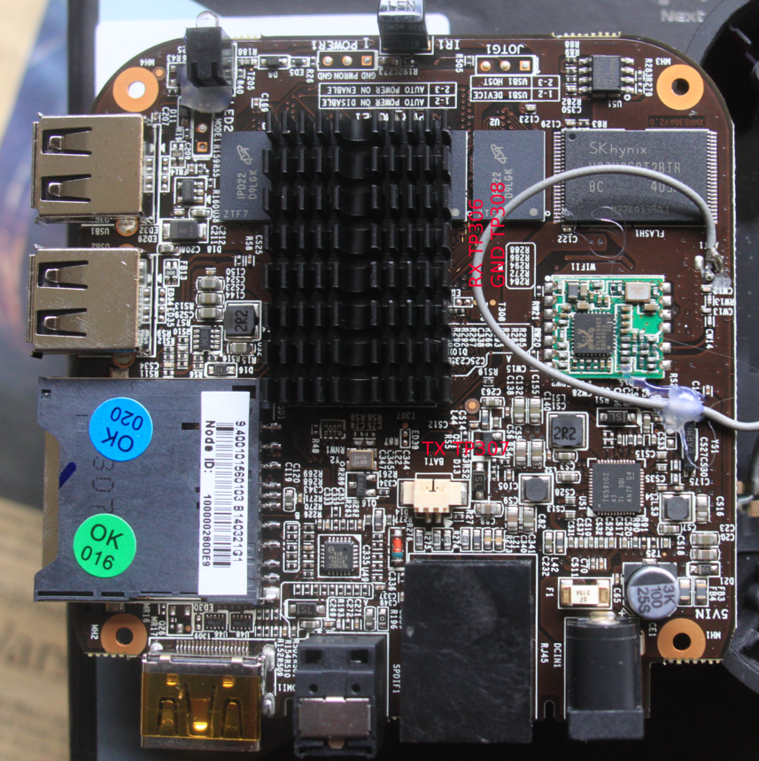
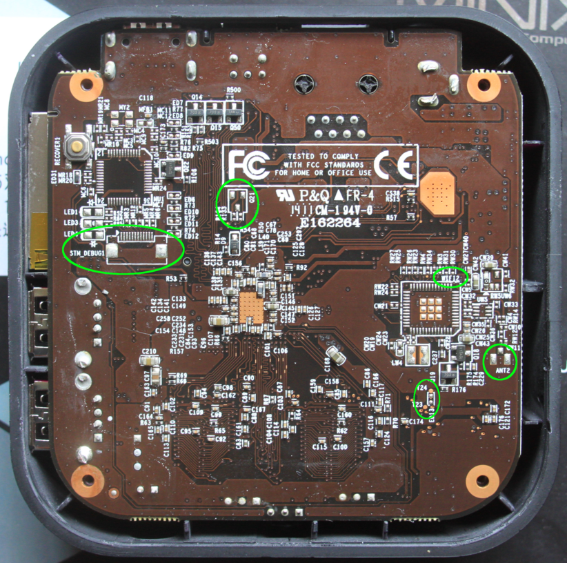
The wifi (rtl8188es) antenna is soldered on, then soldered to an adhesive antenna on the lid, a little awkward, but perfectly reasonable of course. Immediately on the board you can see two missing ICs, one, labelled “WIFI2” is almost certainly Bluetooth, which is not on the x5mini, but is on the x5. More curious though is missing QFP48 IC by the recovery button, and it’s 12 pin “STM_DEBUG” connector. It certainly reminds me of an STM32 footprint, though the debug for cortex-m is normally 10 or 20 pins, not 12? No idea. Two test points on this side, T23 and T24, if it’s indeed a bluetooth module, this is possibly a uart between them? *shrugs*

Back to the “top” side, ethernet is an SMSC LAN8720A, power is a TI T659102, which seems to be pretty common on these boards. There’s two filled jumper blocks with interesting text, “USB1 Device / USB1 Host” and “Auto power on enable/disable” but I’ll leave them for a later time. There’s a rather unexpected battery connector too. Minix doesn’t have any battery backed devices in their catalog, so someone’s design company has been working on this. So much for thinking that minix was an OEM.

T306 is RX, T307 is TX and T308 is GND, for a serial console at 115200, 8N1

minix-neo-x5-mini-pcb-top-notes-30
minix-neo-x5-mini-pcb-bottom-notes-30

Finally, here’s most of the bootup

STM32 Unique ID Register on L1 parts

Last week I mentioned I was seeing duplicate “Unique” ID registers on some STM32L151 parts [1], and included some memory dumps of the three unique ID registers as proof.

However, I had foolishly assumed that on the L1 the Unique ID register was three contiguous 32 bit registers, as it is on the F0, F1, F2, F3 and F4. (The base address changes, but that’s normal and expected)

On the L1, the registers are actually at offset 0, offset 4, and offset 0x14. Thanks for nothing ST! :(
(Oh, and L1 Medium+ and High Density devices use a different base address too, good job)

Here’s some more complete memory dumps for the same three parts I was looking at last week.

UID31:0 UID63:32 UID95:64
Part A 0x0e473233 0x30343433 0x00290031
Part B 0x0e473233 0x30343433 0x00320032
Part C 0x0e473233 0x30343433 0x00380030

Reading other reference manuals, and seeing that the UID registers often have 8 bits of unsigned “Wafer number”, 7 bytes of ASCII Lot number, and 4 bytes of X/Y wafer coordinates in BCD, I would interpret my part “A” above as

Wafer Number Lot Number X/Y coords
Hex 0x0e 0x47323330343433 0x00290031
Natural 0x0e G230443 X=0029, Y=0031

For reference, here are some full dumps of that section of memory. “0x7b747800” is what I had been looking at as UID bits 95:64, note that there are other bits in this section with fixed values, no idea what they mean :)

Part A

(gdb) x /20x 0x1FF80050
0x1ff80050: 0x0e473233  0x30343433  0x7b747800  0x50505091
0x1ff80060: 0x00000011  0x00290031  0x11000000  0x11000011
0x1ff80070: 0x00000000  0x00000000  0x029f067e  0x035a0000
0x1ff80080: 0x035a0000  0x035a0000  0x035a0000  0x035a0000
0x1ff80090: 0x035a0000  0x035a0000  0x035a0000  0x035a0000
(gdb) 

Part B

(gdb) x /20x 0x1FF80050
0x1ff80050: 0x0e473233  0x30343433  0x7b747800  0x50505091
0x1ff80060: 0x00000011  0x00320032  0x11000000  0x11000011
0x1ff80070: 0x00000000  0x00000000  0x02a50685  0x035e0000
0x1ff80080: 0x035e0000  0x035e0000  0x035e0000  0x035e0000
0x1ff80090: 0x035e0000  0x035e0000  0x035e0000  0x035e0000
(gdb)

Part C

(gdb) x /20x 0x1FF80050
0x1ff80050: 0x0e473233  0x30343433  0x7b747800  0x50505091
0x1ff80060: 0x00000011  0x00380030  0x11000000  0x11000011
0x1ff80070: 0x00000000  0x00000000  0x02a50689  0x035e0000
0x1ff80080: 0x035e0000  0x035e0000  0x035e0000  0x035e0000
0x1ff80090: 0x035e0000  0x035e0000  0x035e0000  0x035e0000
(gdb)

[1] Again, these are STM32L151C6T6 parts, revision V, package markings “GH254 VG” and “CHN309”

STM32 Unique ID register not so unique (Or, how to read docs properly)

UPDATE: This post is WRONG! See updated information here

The findings below were based on expecting the UID register to be contiguous as it is on all other STM32 parts. This is not true on the L1 family, and I hadn’t taken enough care with reading the reference manual.

Original post below


Following up from when I wrote about it earlier, it turns out that the “unique” id isn’t as unique as it is meant to be.

On my desk I have three different STM32L151C6T6 revision “V” parts, with exactly the same 96bit unique id. The parts all have package labels “GH254 VG” and CHN309

UID[32:0] (0x1FF80050) UID[63:32] (0x1FF80054) UID[96:64] (0x1FF80058)
Hex 0x0e473233 0x30343433 0x7b747800
Decimal 239546931 808727603 2071230464

According to reports on the irc channel ##stm32, this has also been seen (at least) on stm32f407vet6 parts.

Not fun :(

ID12 RFID breakout board

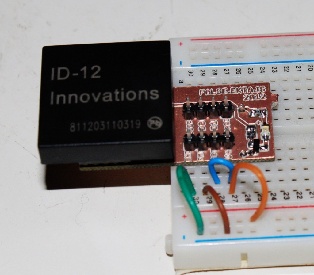
Some time ago I got an ID12 RFID reader module from Sparkfun, during their free day. I had some 2mm socket headers lying around from an xbee project, and finally got around to trying this thing out. Sparkfun sells a “breakout”, but in my mind it’s a bit of a failure, as it takes up too much space for easily mounting on a breadboard.

So, I made my own.
ID12 RFID Breadboard friendly breakout

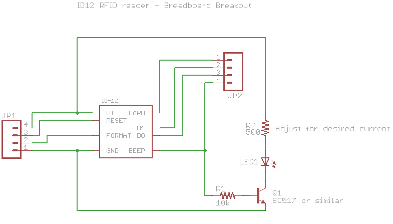
I integrated the LED indicator of a successful read onto the board, and only the useful headers for the ID12 and ID20 modules. It’s much narrower, so easier to use on a breadboard. My board is only ~39mm x 19mm, designed to fit over the channel on a regular breadboard, yet still leave space for plugging wires in. Sparkfun’s is 25mm x 25mm. There’s not much too the design really,

This board was laid out to be made on a milling machine, so there’s no silkscreen text, it’s all in the copper layer instead, and it avoids assuming plated through holes, but it would work just fine manufactured normally. The LED circuit is surface mount, but you can ignore that completely by just not populating those parts.

You can get the eagle files in my github repository

Consider the license to be public domain, or your choice of BSD/MIT/X11.

I’ve only found one RFID card in my wallet that it can actually read, turns out there’s more rfid standards than I thought!

STM32 Device Electronic Signature – Unique Device ID Register

STM32 parts, in all families, have a “Device Electronic Signature” block, which contains a Unique Device ID register of 96 bits. It’s burnt in to the part during manufacture, and is guaranteed to be unique for any device in any context Now, 96 bits is fairly large, and in one application of mine, I need an 8 bit number that reliably varies between devices, and also a 48bit serial number. (Like a MAC address, or EUI48) The canonical way of doing this is to hash the large value to get a small value. I was hoping to use 48 bits of the unique id as “unique enough”

ST doesn’t provide much/any information about what goes into this 96 bit number, but there’s internet rumours that it includes things like wafer x,y position, manufacturing datecodes and so on. If I want something that reliably varies, I need to know a little bit more. I don’t have anything really conclusive, but it looks like I really will have to hash the unique id. Here’s the unique id bits from three STM32F100C8 parts purchased from mouser in the same lot. (Can’t find the order date right now)

device uniqueid[95:64] uniqueid[63:32] uniqueid[31:0]
STM32F100C8-A 0x43023307 0x36314732 0x06E30030
STM32F100C8-B 0x43022507 0x36314732 0x06CF0030
STM32F100C8-C 0x43022407 0x36314732 0x06D10030
STM32F100RB (STM32VL Discovery board) 0x43172128 0x30345532 0x06B30036

On the STM32F0 datasheet, the bits are actually described, and there’s no real reason to assume that it ever changed. They list bits 95:64 as LOT_NUM[55:24], bits 63:40 as LOT_NUM[23:0], bits 39:32 as WAF_NUM[7:0] and bits 31:0 as X and Y coordinates on the wafer expressed in BCD format. That would imply that my three parts in the same box came from the same wafter, but different lot numbers. So, well, maybe it was a different scheme for the F1 :)

Looks like I’ll be hashing anyway then :)