Category Archives: teardown

Vodafone Huawei R216 teardown

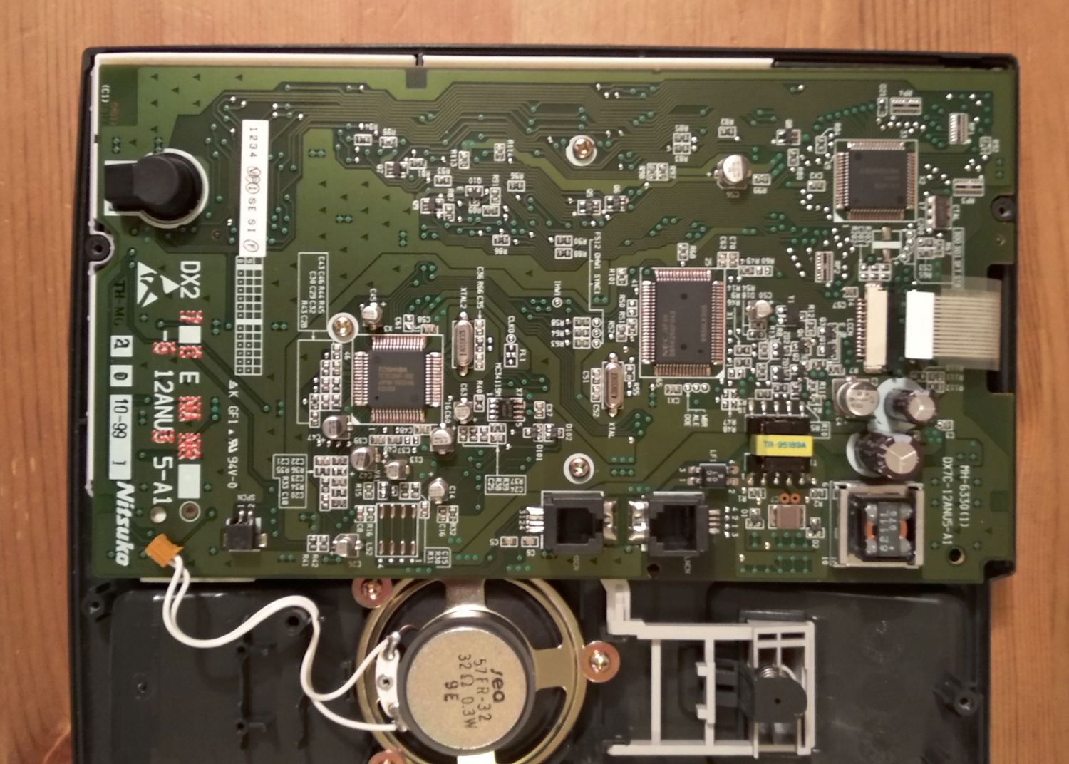
For work reasons, we had a couple of these LTE mobile hotspots deployed permanently. After about two years, they’ve failed, both with puffed up batteries. For no good reason I can think of, the devices don’t work with the battery removed, they just blink constantly. Still, they worked well right up to that point, so, what’s in one? I’ve not tried powering one up again properly, I’m not excited about ordering a spare battery for one, and it’s not (currently) interesting enough to try and provide power to the right place to fake the battery.

You can find the FCC internal photos under QISR216 but it’s blurry. We know it’s from Huawei, but that’s about it. You can also find a GPL compliance tarball that implies it runs android, and has some more details if you’re good at digging into that sort of thing (I’m not really) R216-open resource code.tar.gz

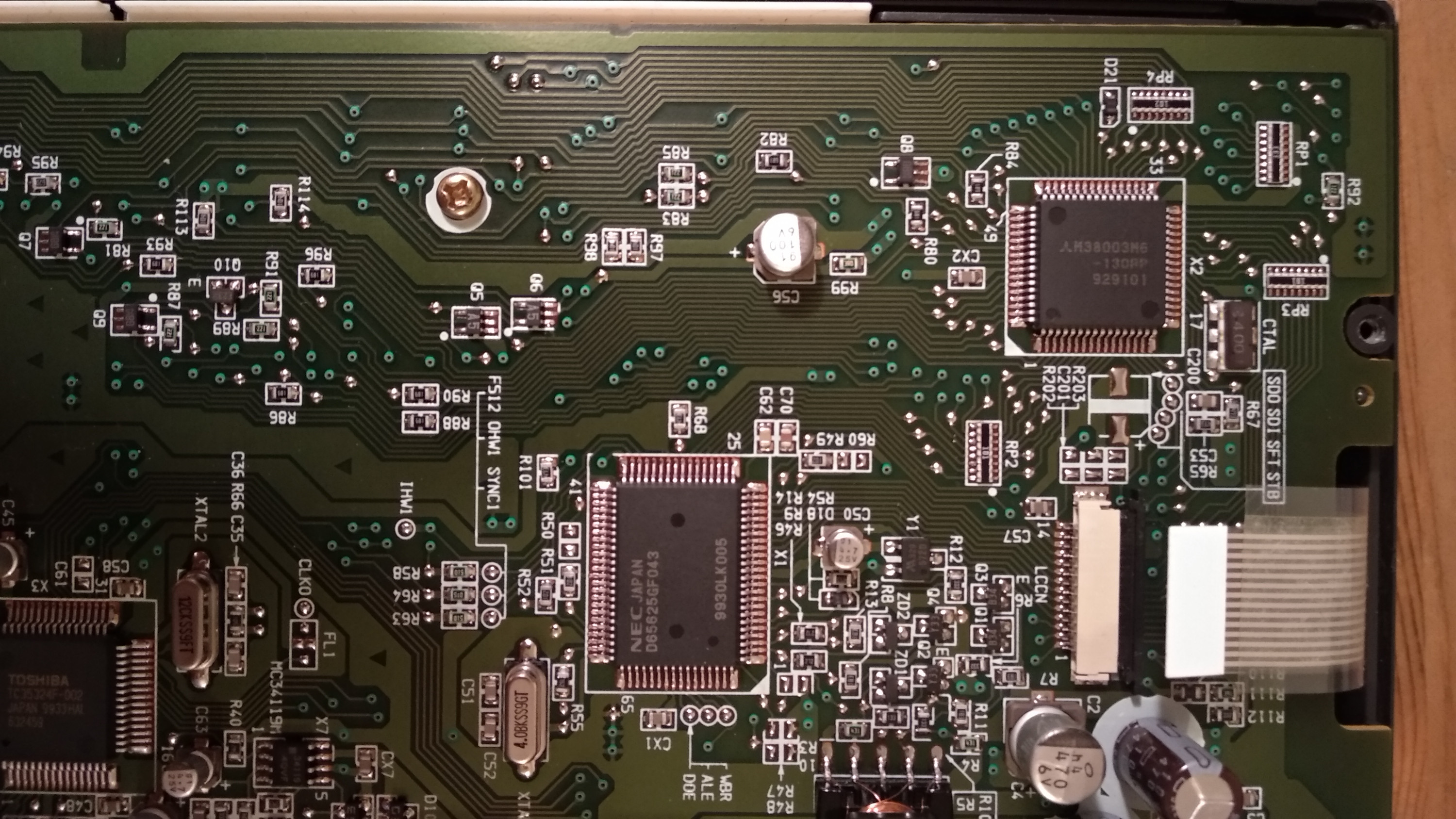
Here’s some photos of it’s guts with a bit of decoding. There’s a few spaces on the PCB for what I suspect is a SD card, and a 5GHz wifi radio, but it’s kinda ugly trawling through old product announcements to see if any of it was ever used. The row of circular pads on the PCB edge are actually available without disassembly, (there’s a row of holes inside the battery compartment that provides access to them), so that’s presumably a “useful” port for something. There’s another set of test pads by the wifi chip.

bcm43241 wifi chipset

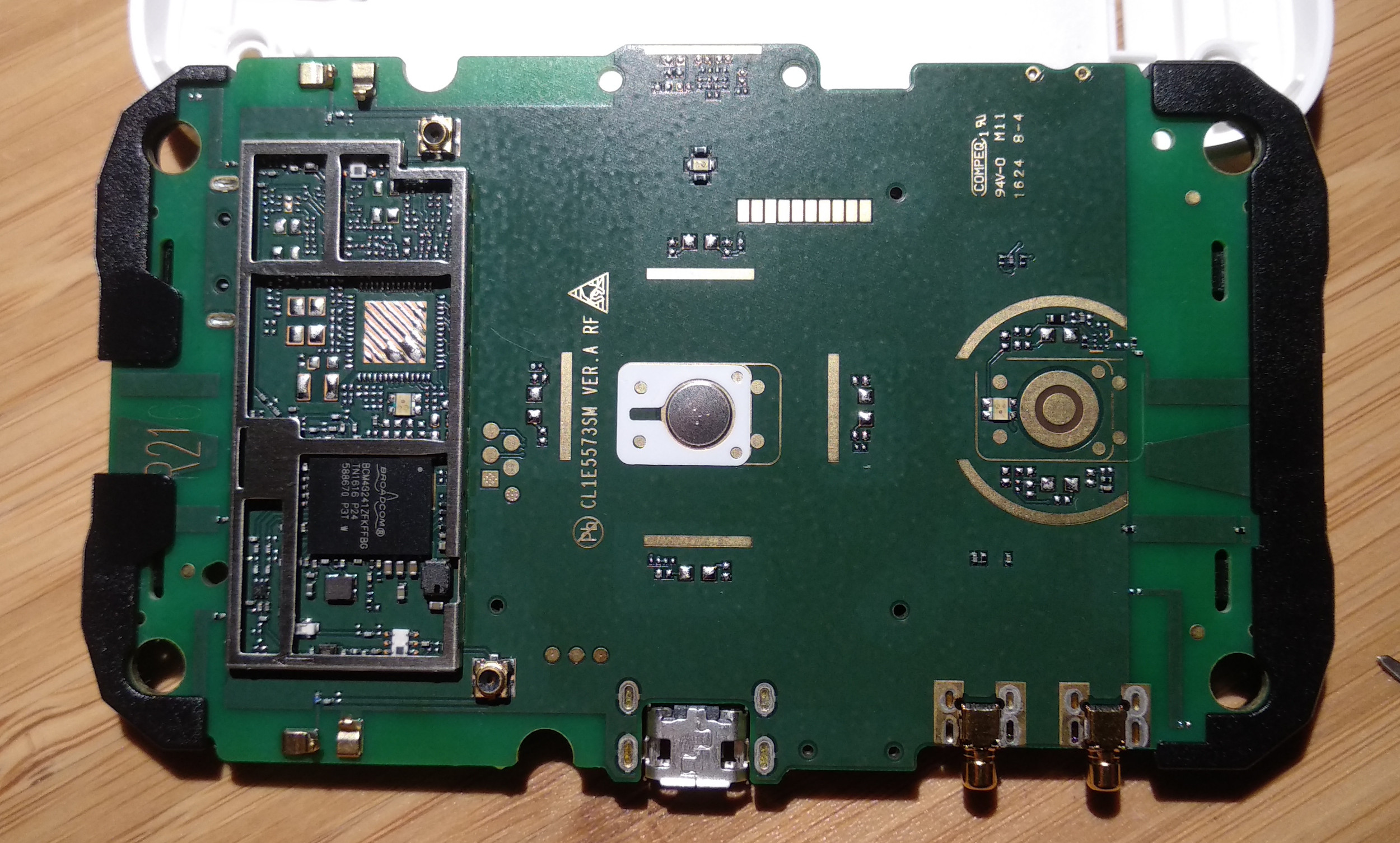
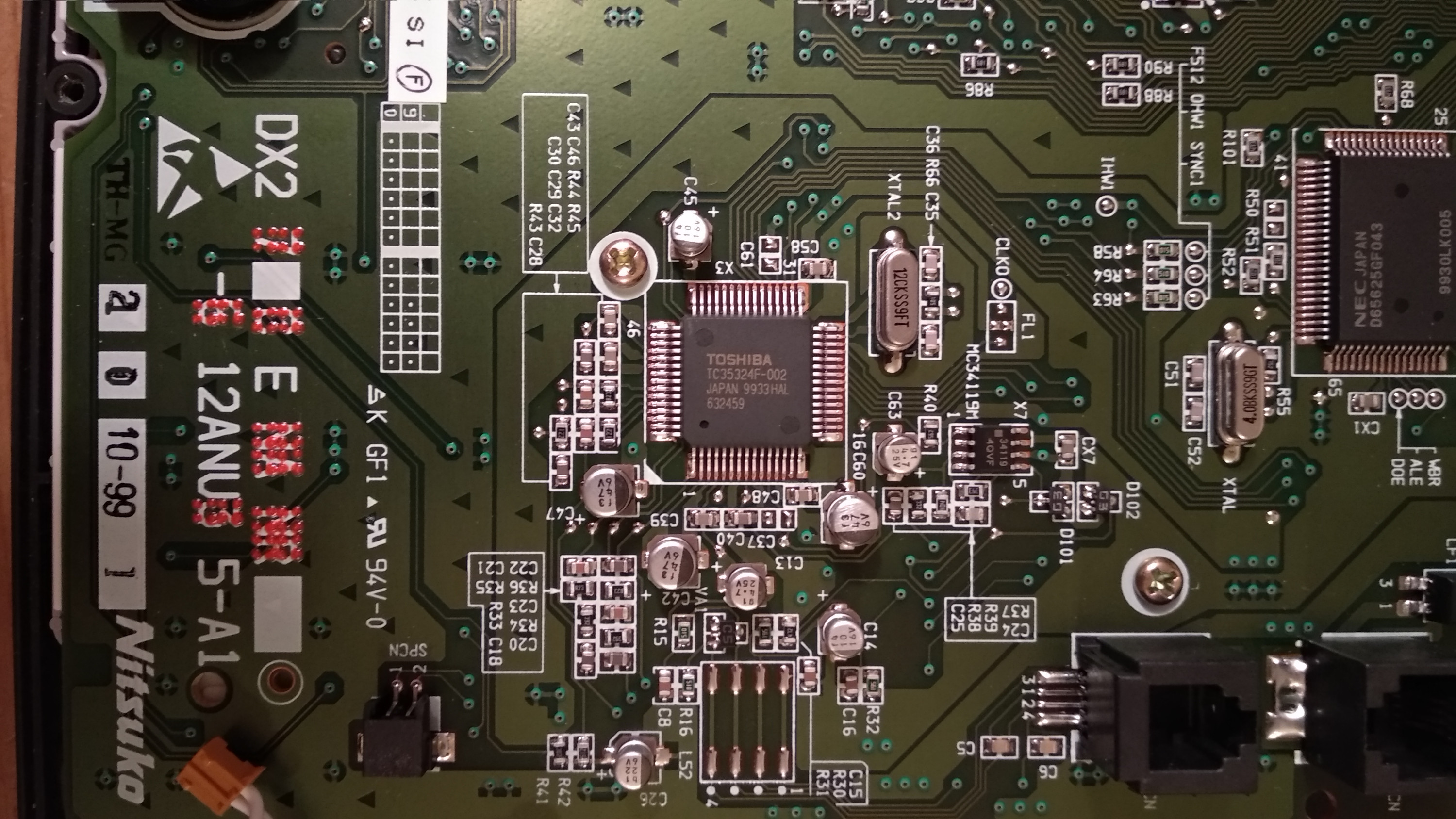
The silver circle in the white field is actually a super slim pushbutton!

And now the “real” side

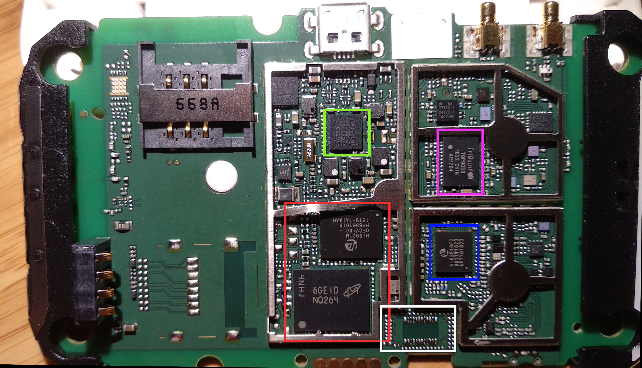
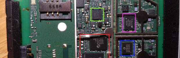
Green is HiSilicon HI6559, a PMIC from reading elsewhere. Red is some Micron flash, and a HiSilicon Hi6921M. You can read a bit more about the part here: https://github.com/Huawei-LTE-routers-mods/README/blob/master/balong_series.md

Blue is HiSilicon Hi6361gfc, presumably the LTE modem? Purple is the Qorvo multiband power amplifier

White box? No idea, not sure what would ever go on that footprint. The blank on the left is presumably a microsd socket.

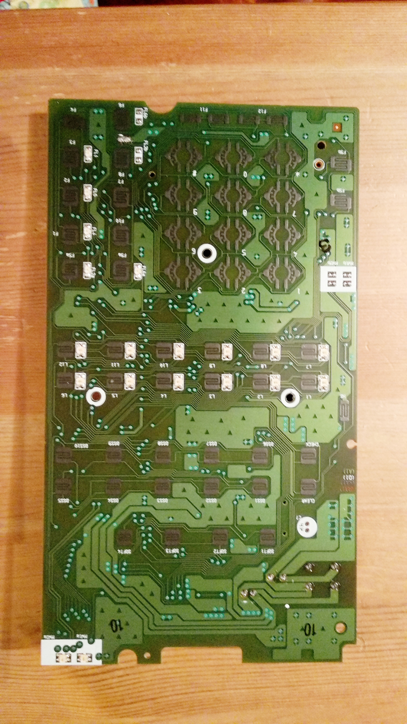
There’s another one of these superslim membrane switches in the top right, between the micro usb and the optional external antenna connectors.

Nitsuka DX2E office phone teardown.

Full model on back of phone: DX2E-12BTXH. Manufactured October 1999. Internal PCB is clearly multi model, and also has the model MH 6330(1) and DX7C-12ANU5-A1
I have a few of these, they’re quite common, you can buy them on ebay for ~$35 or so, or similar models. I had the (very silly, but there was going to be some learning involved) idea of turning one of them into …. a phone. The plan is/was to hookup my own hardware to the handset, buttons and lcd screen, a little linux SoM or similar, and have it run some SIP softphone, running off 18650 batteries. Basically, make a phone…. into a phone. Not all terribly complicated, really.

So, time to open it up. Immediate difficulties are that the entire phone body is a giant PCB with button press pads. I’d loosely been planning on making a little USB HID device to capture all the buttons. (As we’re making a softphone, we don’t need DTMF or anything silly) Gonna have to rethink that now :) Anyway, what’s inside? Super easy to open, plain phillips head screws, no glue, no latches.

Three major ICs, the LCD connector, and the wonderful world of PSTN power supplies.

Let’s start at the top.

X2 is labelled Mitsubishi, M38003M6, and is by all accounts, a mask rom H8/300L series. Part numbers match up for Renesas (the current owner at least) I suspect this is handles all the programmable buttons and the LCD? X1 is a bit of a mystery, it’s labelled NEC D65825GF043. No idea what this is. Custom asic for phones? *shrugs*
Down to the bottom…

X3, Toshiba TC35324F. I found TC35300 and TC35310, both DTMF decoders. I suspect that this listens in on it’s own keypad? Seems a bit excessive though?

X7 (what happened to X4/X5/X6) Is a plain old MC34119. An audio amplifier. The fun things with old tech like this, it talks about being “low current” with only 2.7mA Iq, suitable for batteries :) The datasheet I found even excitedly mentions that it contains 45 active transistors! Whee.

Finally, back side. Just keypads and LEDs really.

Anyway. There it is. Not really sure what next. It wouldn’t be completely unreasonable to just make a whole new pcb that fits under all the button pads, but that’s a lot more than I was planning on. JLPCB and elecrow will make pcbs that big for ~$10 each, but it’s a tedious button pad design. Could do a smaller PCB, only do some of the buttons, just for less hassle, but, meh. Could try and probe up some buttons, lay a big rats nest of wire down. Possibly the easiest way would be to desolder one of the ICs and put something in it’s place, a bunch of selective trace cutting, see if all the buttons go there? Or maybe just look for a different phone altogether…