The Carlo Gavazzi EM210 series [1] of 3 phase energy meters have a rather neat feature. You can mount them on a DIN rail or panel mount, with the same unit, and the display portion is simply detachable, and plugs back in on the reverse side. This is neat tech, and probably saves on inventory in a few distributor places at least, though I don’t imagine it makes any real difference for the end user, who will mount it once and leave it. Still, the display piece has the control buttons and the LCD display, no batteries, and no contacts. So I pulled it apart :)
I don’t know how it works really, it’s presumably the same method as NFC, by modulating the power draw from a capacitively or inductively coupled connection. It’s cool though. ATMega169 for the LCD control and buttons. Not entirely sure what the crystal is for, it’s marked “KDS3C” but I didn’t look further for a speed marking. Presumably you need a proper crystal to be able to synchronize the coupled connection properly? I don’t believe it’s an RTC crystal, as this is the detachable display portion. I always like seeing cutouts mid PCB for inserting big components.
The trimpot is an interesting idea. It’s used as a “lock”. With it turned all the way one way, the device is considered locked, and this screw access is on the back of the display portion. This portion also has tags for tamper seals, so I guess that’s one way of doing it on the cheap? Presumably just an ADC input to determine lock status.
The oddly slanted through hole parts on the left are the front panel buttons, nice alignment :)
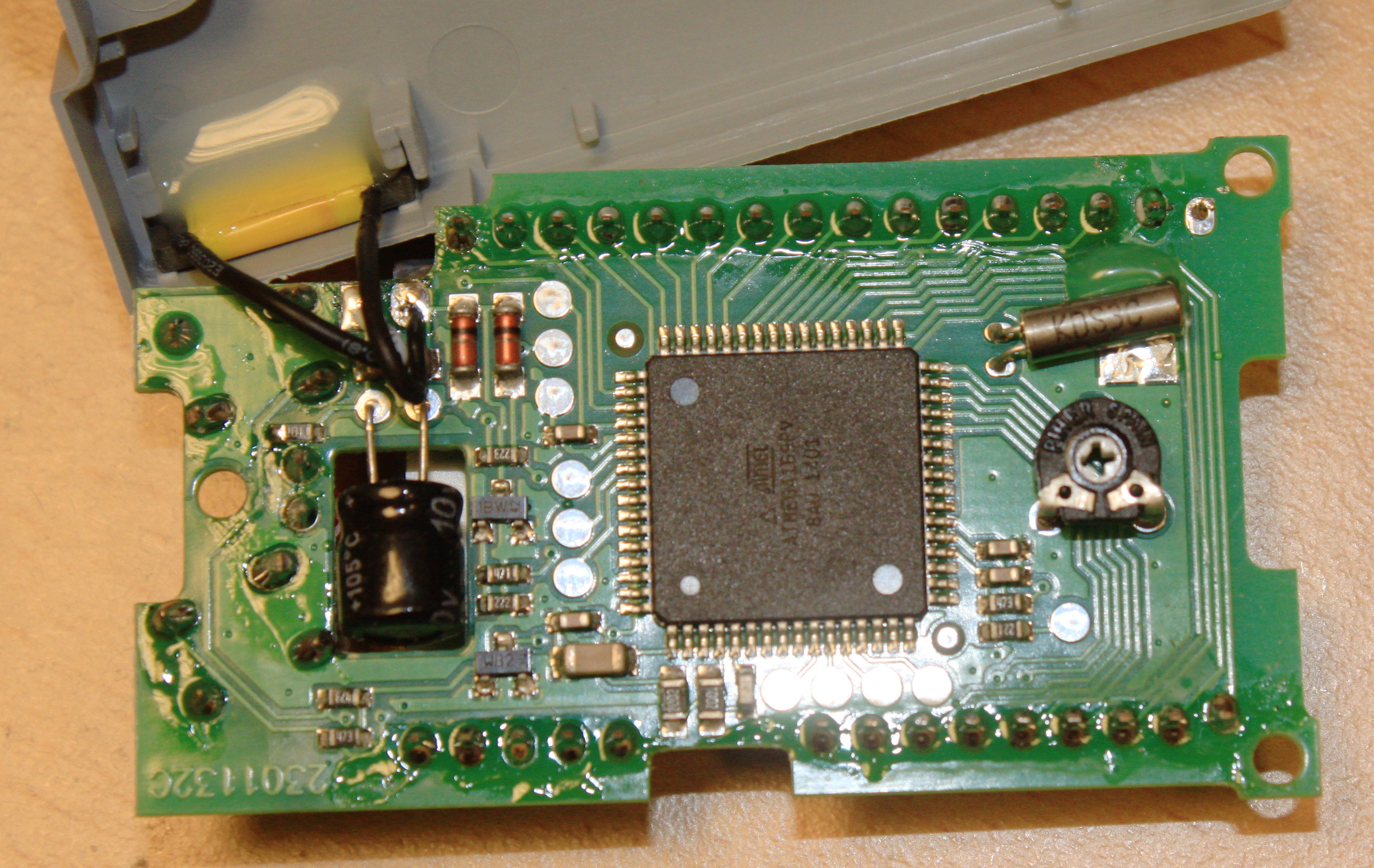
ATMega169 for LCD control, coupled connection
[1] I’d link to them, but their website is junk and doesn’t let you link to products, and requires sign up to get a datasheet, that uses old names. The same sort of stupid games with redirecting you to different websites for different markets for the same device and all the usual terrible product management choices that lead engineers to ignore your products.